Device ESD Sensitivity Testing
Introduction
Semiconductor devices are susceptible to static discharges to varying degrees. These devices have been becoming more sensitive to Electrostatic Discharge (ESD) since the mid 1990’s. The ESD Association (ESDA) has published a Roadmap for semiconductor devices. Figure 1 shows the ESD sensitivity trend for Human Body Model (HBM) sensitive devices. The ESDA roadmap also contains trends for Charged Device Model (CDM).

Figure 1 – HBM Trend Chart
These ESD sensitivity trends are having a dramatic impact on any activity where unprotected ESD sensitive devices are handled. Some factories have experienced significant yield losses due to ESD damage. In some cases, the factory was aware of the device sensitivity and simply assumed that that the installed ESD controls were adequate. In others, ESD sensitive devices were introduced without the user’s knowledge. In both cases, ESD damage could have been prevented if:
- The device ESD sensitivity was known and
- The user of the device had the knowledge necessary to install an ESD control program designed to protect the devices.
These are two vitally important but separate requirements. This whitepaper will address device ESD sensitivity testing.
Device ESD Sensitivity Testing Standards
The ESD Association has published a number of documents that describe how to determine the ESD sensitivity of devices to various discharge models. The following is a list of the primary test standards that relate to the handling of devices in a factory, lab or field service setting.
- ANSI/ESDA/JEDEC JS-001-2017 – Human Body Model (HBM) – component level testing
- ANSI/ESDA/JEDEC JS-002-2018 – Charged Device Model (CDM) – component level testing
Note: this test method charges the device under test with a static field. A device lead is then grounded in the presence of the field.
- ESD SP5.2-2019 – Machine Model (MM) – component level
Note: This document was initially an ESDA standard but it’s use is no longer being recommended since similar information can be obtained using the HBM test method. The document has been demoted to Standard Practice status.
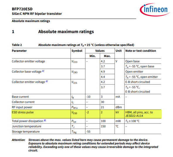
Semi-conductor manufacturers use the test standards during their product qualification testing process. However, even though the data has been collected it is difficult, if not impossible, to obtain this data unless you are preferred customer. Searching the semiconductor manufacturer’s website sometimes yields results such as the data sheet shown in Figure #2. Unfortunately, the referenced data sheet only shows values for the HBM test method. The manufacturer either did not test for CDM and MM or the information was not included in the data sheet. In either case, information that is vital to the user of these components is not available. Internet searches for ESD sensitivity data sheets (when found) will find a high percentage will provide HBM sensitivity data. A much smaller percentage will find MM and CDM data in almost equal numbers.

Figure 2 – Data Sheet
Impact on ESD Processes
So, what can the user do? There are two options. First, implement ESD control standards such as ANSI/ESD S20.20 or IEC 61340-5-1. If the requirements in either of these documents are followed, the user can claim that their process is capable of handling devices with the following sensitivity:
- HBM – 100 volts or higher
- CDM – field induction – 200 volts or higher
- MM – 35 volts or higher
The use of either of these standards will protect the vast majority of devices from ESD damage. The only problem with this approach occurs when a more sensitive device is introduced into the process. If the ESD sensitivity of this new device is known the limits in the standards can be adjusted accordingly. As an example, let’s look at HBM from a process capability point of view. The limit in ANSI/ESD S20.20 of 35 megohms for wrist straps will keep a person’s maximum voltage while moving to less than 100 volts. Figure 3 shows data on wrist strap grounding. If a 50-volt HBM device is introduced into your process, the device will be protected from damage since an operator wearing a properly grounded wrist strap will have a resistance to ground in the 1-10 megohm range. This keeps their body voltage to less than 40 volts.

Figure 3 – Body Voltage vs. Resistance to Ground for Wrist straps
The situation is more complicated when it comes to the grounding of personnel through a footwear / flooring system. The body voltages cannot be pre-determined and body voltage data must be generated using test method ANSI/ESD STM 97.2.
A similar situation occurs with CDM. ANSI/ESD S20.20 limits the static fields for unprotected ESDS that are in direct contact (or closer than 2.5 cm) to less than 125 volts / inch. Adhering to these limits will protect devices that have a CDM sensitivity of 200 volts or higher. If presented with a device with a lower CDM sensitivity, the maximum allowable field should be set for ½ the CDM sensitivity value if the device will be in contact with the charged insulator or less than 2.5 cm from the item. As an example, if a device’s CDM sensitivity is 50 volts the maximum allowable static field should be set at 25 volts per inch.
Determining ESD Device Sensitivity
If you do not know the ESD sensitivity of your devices and cannot get the information from the device supplier or are experiencing unacceptable electrical fallout, then you might want to consider purchasing equipment so that you can perform your own testing. There are a number of suppliers that can provide testing equipment. Testers can provide manual or fully automatic testing modes and can range in price from 10’s to hundreds of thousands of dollars for EACH ESD testing model. Data from these various testers can be used to prepare device data sheets.
This cost makes device testing prohibitive for many companies. Prostat Corporation has developed a low cost HBM simulator that can be used to test devices in compliance with ANSI/ESDA/JEDEC JS-001. The Prostat PDS-510 meets the waveform requirements of this standard. Unlike most commercial testers that come with a test head, the Prostat PDS-510 is a two-pin tester. This means that the device under test must be connected to each of the two pins that are being tested. If there are multiple pins that must be tested the user of the PDS-510 must design a way to connect to the pins under test AND the user must have a way to test the device after HBM discharges to check for damage. Data collected using the PDS-510 can be used for data sheet reporting.
The benefit of the PDS-510 is that in addition to being low cost it is portable and can be run on built-in batteries. The unit also has a precision built-in DC power supply that can be used to charge items up to 4,000 VDC.
ESD Process Analysis
The types of actual ESD discharges found in a process can vary widely. Discharges into a device can come from people (HBM) or charged conductors (MM/CDM). Discharges from a device are typically CDM but a more energetic discharge can be seen if the ESD sensitive device is mounted to a printed circuit board (PCBA). In this situation, the entire board can become charged and a discharge can also contain energy from the entire board (not just the device). This discharge is called a Charged Board Event or CBE.
During actual process assessments, where the ESD sensitivity of devices was NOT known, it was discovered that the PDS-510 can be used to deliver other ESD discharge models to devices under test. The PDS-510 has been used in multiple ESD investigations to help customers get a general indication of the ESD sensitivity of a device. As mentioned above, the PDS-510 meets the requirements of ANSI/ESD ESDA/JEDEC JS-001. HBM test data can be used for data sheet reporting.
Alternate Testing Procedures
The following test procedure defines a methodology to provide the user with a general indication of the ESD sensitivity of the item under test.
Part A – external discharges to the item under test
ESD Models – Machine Model and External Charged Device Model Pulse
Machine Model is related to the Human Body Model in that when a device is subjected to either discharge model the failure site on the ESDS is similar. The difference between the models is the voltage that it takes to cause damage. The Machine Model is much more damaging to devices then the Human Body Model. Studies have shown that MM ESD sensitivity values are 10-30 times lower than the HBM values. As an example, if a device had an HBM sensitivity of 1,000 volts the calculated MM sensitivity would likely be between 30 and 100 volts. Figure 4 is an excerpt from the Industry ESD Council’s White Paper #1.

Figure 4 – HBM to MM Correlation
If, however, the HBM values are not known or if the user wants to better understand the device MM sensitivity the PDS-510 can be used.
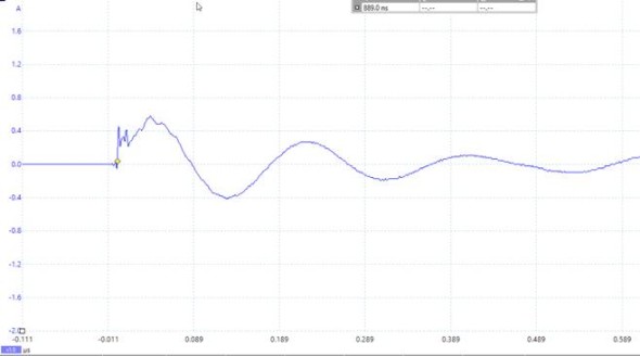
Machine Model pulses come from a conductive object that has a relatively high capacitance (200pf). The following example shows one approach that has been successfully used. Figure 5 shows the test setup with a specially designed test board. Figure 6 shows the MM waveform that is delivered to the device under test.

Figure 5 – Test Setup for MM Pulse using PDS-510

Figure 6 – MM Pulse from Test Board
Machine Model Test Procedure:
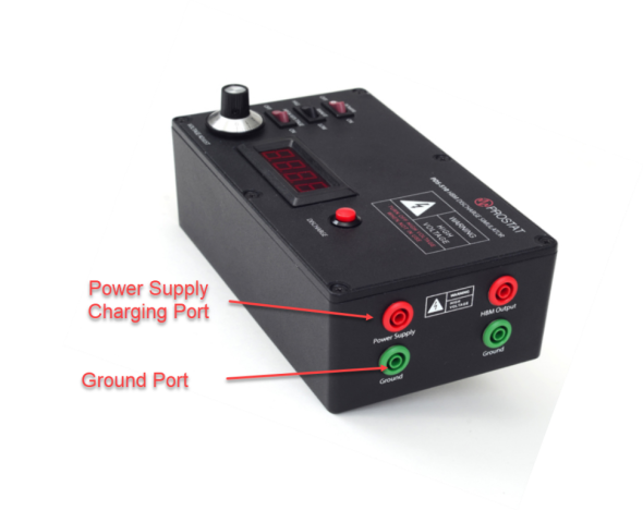
- Connect the PDS-510 to a known AC ground through either of the two ground ports. (Figure 7)
- Connect a second lead from the PDS-510 ground port to the metal plate in order to ground it.
- Place the conductive test board onto the metal plate. Care must be taken to ensure that the conductive traces on the test board do not contact the grounded metal plate.
- Connect a lead to the red power supply port. The red lead must not come into contact with ground.
- Turn on the PDS-510 and dial in the desired test voltage.
- Using the charging lead, charge the conductive trace of the test board.
- Discharge the test board into the device/circuit under test.
- Check the device for continued function.
- If no change to the device is found increase the power supply voltage and repeat steps 6-8 until the device fails to meet specification.

Figure 7 – PDS-510 Connections
Charged Device Model Procedure:
This procedure is similar to the MM test with the exception that the grounded metal plate is not used. It is important to understand that this is NOT your typical CDM test. Charged Device Model testing, as described by the name, usually involves the grounding of a charged device which is charged by a static field. ANSI/ESDA/JEDEC JS-002 exposes the device under test to a field which charges the device. A charged pin is then grounded and the device under test is checked for damage. The test described here is not field induced CDM but a CDM pulse that is injected into the device under test from an outside charged source.
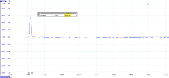
The setup and test procedure is similar to the MM test. The only difference is that the ground lead attached to the metal plate is removed. This changes the capacitance of the test board and allows the delivery of a CDM pulse to the device under test. Figure 8 shows a CDM discharge from the test board. The conductive traces of the test board are charged using the PDS-510 power supply.

Figure 8 – CDM Pulse from Test Board
Part B – CDM Testing using PSD-510
This procedure simulates the test setup of ANSI/ESDA/JEDEC JS-002-2018. Under this procedure the device under test is placed onto a metal plate (that is isolated from ground) that is covered with a thin dielectric material (0.4mm thick). The metal plate is charged to a known voltage. This causes the device under test to charge by the resulting field. A grounded lead then discharges the pin being tested. In this procedure the pins are manually discharged with a grounded lead. After the discharge the device is functionally checked to see if damage has occurred. If no damage is found the PDS-510 voltage is increased and the process is repeated until damage is found.

Figure 9 – Field Induced CDM Test Setup
Conclusion
In order to know that an installed ESD process is capable of protecting ESD sensitive devices it is imperative that the value of the most ESD sensitive devices are known. At a minimum, information related to HBM, MM and CDM are required. If this information is available steps can be taken to check the process and modify it as required.
However, if the required ESD sensitivity information is not available and the supplier cannot provide the test data it is possible to get a good approximation of the device sensitivity using Prostat’s PDS-510. This unit and the approach documented in this whitepaper have worked to resolve ESD fallout in multiple factories.
Recent Comments